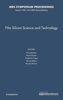
Film Silicon Science and Technology
Herausgeber: Stradins, Paul; Finger, Friedhelm; Boukai, Akram
Film Silicon Science and Technology
Herausgeber: Stradins, Paul; Finger, Friedhelm; Boukai, Akram
- Gebundenes Buch
- Merkliste
- Auf die Merkliste
- Bewerten Bewerten
- Teilen
- Produkt teilen
- Produkterinnerung
- Produkterinnerung
Symposium A, 'Film Silicon Science and Technology', was held April 1-5, 2013 at the 2013 MRS Spring Meeting in San Francisco, California.
Andere Kunden interessierten sich auch für
![Amorphous and Plycrystalline Thin-Film Silicon Science and Technology - 2008 Amorphous and Plycrystalline Thin-Film Silicon Science and Technology - 2008]() Amorphous and Plycrystalline Thin-Film Silicon Science and Technology - 2008117,99 €
Amorphous and Plycrystalline Thin-Film Silicon Science and Technology - 2008117,99 €![Amorphous and Polycrystalline Thin-Film Silicon Science and Technology - 2010 Amorphous and Polycrystalline Thin-Film Silicon Science and Technology - 2010]() Amorphous and Polycrystalline Thin-Film Silicon Science and Technology - 2010117,99 €
Amorphous and Polycrystalline Thin-Film Silicon Science and Technology - 2010117,99 €![Materials Issues in Applications of Amorphous Silicon Technology Materials Issues in Applications of Amorphous Silicon Technology]() Materials Issues in Applications of Amorphous Silicon Technology36,99 €
Materials Issues in Applications of Amorphous Silicon Technology36,99 €![Impurity Diffusion and Gettering in Silicon Impurity Diffusion and Gettering in Silicon]() Impurity Diffusion and Gettering in Silicon35,99 €
Impurity Diffusion and Gettering in Silicon35,99 €![Thin Film Materials Thin Film Materials]() Ben FreundThin Film Materials94,99 €
Ben FreundThin Film Materials94,99 €![Gate Stack and Silicide Issues in Silicon Processing Gate Stack and Silicide Issues in Silicon Processing]() Gate Stack and Silicide Issues in Silicon Processing35,99 €
Gate Stack and Silicide Issues in Silicon Processing35,99 €![Advances in Gan, GAAS, Sic and Related Alloys on Silicon Substrates Advances in Gan, GAAS, Sic and Related Alloys on Silicon Substrates]() Advances in Gan, GAAS, Sic and Related Alloys on Silicon Substrates35,99 €
Advances in Gan, GAAS, Sic and Related Alloys on Silicon Substrates35,99 €-
-
-
Symposium A, 'Film Silicon Science and Technology', was held April 1-5, 2013 at the 2013 MRS Spring Meeting in San Francisco, California.
Produktdetails
- Produktdetails
- Verlag: Cambridge University Press
- Seitenzahl: 238
- Erscheinungstermin: 16. Januar 2014
- Englisch
- Abmessung: 235mm x 157mm x 17mm
- Gewicht: 501g
- ISBN-13: 9781605115139
- ISBN-10: 1605115134
- Artikelnr.: 39761911
- Herstellerkennzeichnung
- Libri GmbH
- Europaallee 1
- 36244 Bad Hersfeld
- gpsr@libri.de
Part I. Thin Film Silicon Solar Cells: 1. Light management using periodic
textures for enhancing photocurrent and conversion efficiency in thin-film
silicon solar cells; 2. Panasonic's thin film silicon technologies for
advanced photovoltaics; 3. Hydrogen-plasma etching of thin amorphous
silicon layers for heterojunction interdigitated back-contact solar cells;
4. Employing lc-SiOX:H as n-type layer and back TCO replacement for
high-efficiency a-Si:H/lc-Si:H tandem solar cells; 5. A vertical PN
junction utilizing the impurity photovoltaic effect for the enhancement of
ultra-thin film silicon solar cells; 6. Impact on thin film silicon
properties and solar cell parameters of texture generated by laser
annealing and chemical etching of ZnO:Al; 7. Novel intermediate reflector
layer for optical and morphological tuning in the micromorph thin film
tandem cell; 8. Development of nanocrystalline silicon based multi-junction
solar cell technology for high volume manufacturing; 9. SnO2:F with very
high haze value and transmittance in near infrared wavelength for use as
front transparent conductive oxide films in thin-film silicon solar cells;
Part II. Novel Silicon-Based Devices and Solar Cells: 10. Amorphous silicon
based betavoltaic devices; 11. SiC monolithically integrated wavelength
selector with 4 channels; 12. Design of an optical transmission WDM link
using plastic optical fibers; 13. Optoelectronic logic functions using
optical bias controlled SiC multilayer devices; 14. Improvement of seed
layer smoothness for epitaxial growth on porous silicon; Part III.
Materials and Devices Characterization and Simulation: 15. Local junction
voltages and radiative ideality factors of a-Si:H solar modules determined
by electroluminescence imaging; 16. The dependence of the crystalline
volume fraction on the crystallite size for hydrogenated nanocrystalline
silicon based solar cells; 17. Carrier lifetime measurements by
photoconductance at low temperature on passivated crystalline silicon
wafers; 18. Characterization of boron doped amorphous silicon films by
multiple internal reflection infrared spectroscopy; 19. Emission spectra
study of plasma enhanced chemical vapor deposition of intrinsic, n1, and p1
amorphous silicon thin films; 20. On the origin of the Urbach Rule and the
Urbach Focus; 21. Ultrafast optical measurements of acoustic phonon
attenuation in amorphous and nanocrystalline silicon; 22. Stress analysis
of free-standing silicon oxide films using optical interference; 23. Effect
of RF or VHF plasma on nanocrystalline silicon thin film structure: insight
from OES and Langmuir Probe measurements; Part IV. Defects and Transport:
24. Defect densities and carrier lifetimes in oxygen doped nanocrystalline
Si; 25. Microstructure characterization of amorphous silicon films by
effusion measurements of implanted helium; 26. Temperature dependence of
1/f noise and electrical conductivity measurements on p-type a-Si:H
devices; 27. Study of surface passivation of CZ c-Si by PECVD a-Si:H films:
a comparison between quasi-steady-state and transient photoconductance
decay measurement; Part V. Nanostructured Silicon and Related Novel
Materials: 28. Charge transport in nanocrystalline germanium/hydrogenated
amorphous silicon mixed-phase thin films; 29. Low temperature annealing of
inkjet-printed silicon thin-films for photovoltaic and thermoelectric
devices; 30. Shape evolution of faceted silicon nanocrystals upon thermal
annealing in an oxide matrix; 31. Crystallization kinetics of
plasma-produced amorphous silicon nanoparticles.

