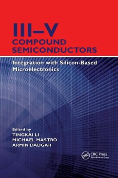
III-V Compound Semiconductors
Integration with Silicon-Based Microelectronics
Herausgeber: Li, Tingkai; Dadgar, Armin; Mastro, Michael
III-V Compound Semiconductors
Integration with Silicon-Based Microelectronics
Herausgeber: Li, Tingkai; Dadgar, Armin; Mastro, Michael
- Broschiertes Buch
- Merkliste
- Auf die Merkliste
- Bewerten Bewerten
- Teilen
- Produkt teilen
- Produkterinnerung
- Produkterinnerung
A discussion of recent advances, this book covers the scientific and technological exploration of the applications, properties, and processes of GaN, GaAs, and other III-V compound semiconductor devices within Si-based technology. It includes a broad range of topics, from fundamental material properties and materials integration to demonstration and industrial devices. The book also contains discussions of materials and devices, including their basic physical and chemical properties, their mechanisms, how to measure their properties, and how to fabricate them.
Andere Kunden interessierten sich auch für
![III-V Compound Semiconductors III-V Compound Semiconductors]() III-V Compound Semiconductors266,99 €
III-V Compound Semiconductors266,99 €![Compound Semiconductors 2002 Compound Semiconductors 2002]() Marc IlegemsCompound Semiconductors 2002569,99 €
Marc IlegemsCompound Semiconductors 2002569,99 €![Quaternary Alloys Based on III-V Semiconductors Quaternary Alloys Based on III-V Semiconductors]() Vasyl TomashykQuaternary Alloys Based on III-V Semiconductors60,99 €
Vasyl TomashykQuaternary Alloys Based on III-V Semiconductors60,99 €![Multinary Alloys Based on III-V Semiconductors Multinary Alloys Based on III-V Semiconductors]() Vasyl TomashykMultinary Alloys Based on III-V Semiconductors59,99 €
Vasyl TomashykMultinary Alloys Based on III-V Semiconductors59,99 €![Quaternary Alloys Based on III-V Semiconductors Quaternary Alloys Based on III-V Semiconductors]() Vasyl TomashykQuaternary Alloys Based on III-V Semiconductors229,99 €
Vasyl TomashykQuaternary Alloys Based on III-V Semiconductors229,99 €![Atomic Diffusion in III-V Semiconductors Atomic Diffusion in III-V Semiconductors]() Brian TuckAtomic Diffusion in III-V Semiconductors74,99 €
Brian TuckAtomic Diffusion in III-V Semiconductors74,99 €![Dopants and Defects in Semiconductors Dopants and Defects in Semiconductors]() Matthew D. McCluskeyDopants and Defects in Semiconductors232,99 €
Matthew D. McCluskeyDopants and Defects in Semiconductors232,99 €-
-
-
A discussion of recent advances, this book covers the scientific and technological exploration of the applications, properties, and processes of GaN, GaAs, and other III-V compound semiconductor devices within Si-based technology. It includes a broad range of topics, from fundamental material properties and materials integration to demonstration and industrial devices. The book also contains discussions of materials and devices, including their basic physical and chemical properties, their mechanisms, how to measure their properties, and how to fabricate them.
Produktdetails
- Produktdetails
- Verlag: CRC Press
- Seitenzahl: 604
- Erscheinungstermin: 23. September 2019
- Englisch
- Abmessung: 234mm x 156mm x 32mm
- Gewicht: 904g
- ISBN-13: 9780367383268
- ISBN-10: 0367383268
- Artikelnr.: 57816434
- Herstellerkennzeichnung
- Libri GmbH
- Europaallee 1
- 36244 Bad Hersfeld
- gpsr@libri.de
Tingkai Li, Ph.D., is currently working at Micron Technology, Inc. as a senior technical member. He published over 100 technical papers, edited three preceding books, and was granted 93 US patents and many awards related in semiconductor and compound semiconductor device and materials research. He is an invited paper reviewer of the Applied Physics Letter, Journal of Applied Physics, IEEE Electron Device Letter, IEEE Transaction of Electron Device, etc., and overseas editor of Journal of Inorganic Materials. He is also honorary professor at Hunan University, Wuhan University of Technologies, and Zhejiang University in China. Dr. Li received a Ph.D. degree in Materials Science and Engineering from Zhejiang University, P. R. China, in 1987, and was a postdoctoral fellow and research scientist at Virginia Polytechnic Institute and State University, Blacksburg, Virginia from 1989-1995. From 1995-1998, he worked as a Staff Scientist in EMCORE Cooperation, New Jersey. He joined Sharp Laboratories in 1998 as a principal member of technical staff and project manager. Michael Mastro, currently a civilian staff scientist at the U.S. Naval Research Lab, has more than 10 years of research experience in thin film growth and characterization, as well as semiconductor device design and nano-fabrication. This includes a number of fundamental advances in the fabrication of planar LEDs and high-power electronic devices, in addition to the development of novel nano-devices, which has resulted in authorship on more than 100 papers and patents. Michael earned a Ph.D. from the University of Florida in 2001 and a B.S. in Chemical Engineering from the Johns Hopkins University in 1997. Armin Dadgar studied physics at University of Heidelberg and at TU-Berlin, where he received his doctor of natural sciences in 1999, successfully developing an alternative method to Fe doping to obtain semiinsulating InP b
Part I: Basic Physical and Chemical Properties Fundamentals and the Future
of Semiconductor Device Technology. The Challenge of III-V Materials
Integration with Si Microelectronics.
Part II: GaN and Related Alloys on Silicon Growth and Integration
Techniques III-Nitrides on Si Substrate. New Technology Approaches.
Part III: III-V Materials and Device Integration Processes with Si
Microelectronics Group III-A Nitrides on Si: Stress and Microstructural
Evolution. Direct Growth of III-V Devices on Silicon. Optoelectronic Device
Integrated on Si. Reliability of III-V Electronic Devices.
Part IV: Defect and Properties Evaluation and Characterization In Situ
Curvature Measurements, Strains, and Stresses in the Case of Large Wafer
Bending and Multilayer Systems. X-Ray Characterization of Group
III-Nitrides. Luminescence in GaN.
Part V: Device Structures and Properties GaN-Based Optical Devices on
Silicon. The Conventional III-V Materials and Devices on Silicon III-V
Solar Cells on Silicon.

