Sima Dimitrijev
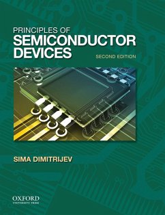
Principles of Semiconductor Devices
Sima Dimitrijev
Principles of Semiconductor Devices
- Gebundenes Buch
- Merkliste
- Auf die Merkliste
- Bewerten Bewerten
- Teilen
- Produkt teilen
- Produkterinnerung
- Produkterinnerung
The dimensions of modern semiconductor devices are reduced to the point where classical semiconductor theory, including the concepts of continuous particle concentration and continuous current, becomes questionable. Further questions relate to two-dimensional transport in the most important field-effect devices and one-dimensional transport in nanowires and carbon nanotubes. Designed for upper-level undergraduate and graduate courses, Principles of Semiconductor Devices, Second Edition, presents the semiconductor-physics and device principles in a way that upgrades classical semiconductor…mehr
Andere Kunden interessierten sich auch für
![Introduction to Semiconductor Physics and Devices Introduction to Semiconductor Physics and Devices]() Mykhaylo EvstigneevIntroduction to Semiconductor Physics and Devices38,99 €
Mykhaylo EvstigneevIntroduction to Semiconductor Physics and Devices38,99 €![Quantum Transport in Semiconductor Devices Quantum Transport in Semiconductor Devices]() David K FerryQuantum Transport in Semiconductor Devices177,99 €
David K FerryQuantum Transport in Semiconductor Devices177,99 €![Nanoscale Semiconductor Devices Nanoscale Semiconductor Devices]() Nanoscale Semiconductor Devices123,99 €
Nanoscale Semiconductor Devices123,99 €![Transport in Semiconductor Mesoscopic Devices (Second Edition) Transport in Semiconductor Mesoscopic Devices (Second Edition)]() David K FerryTransport in Semiconductor Mesoscopic Devices (Second Edition)114,99 €
David K FerryTransport in Semiconductor Mesoscopic Devices (Second Edition)114,99 €![Introduction to Semiconductor Physics and Devices Introduction to Semiconductor Physics and Devices]() Mykhaylo EvstigneevIntroduction to Semiconductor Physics and Devices38,99 €
Mykhaylo EvstigneevIntroduction to Semiconductor Physics and Devices38,99 €![Sub-Micron Semiconductor Devices Sub-Micron Semiconductor Devices]() Sub-Micron Semiconductor Devices186,99 €
Sub-Micron Semiconductor Devices186,99 €![The Physics of Semiconductor Devices The Physics of Semiconductor Devices]() The Physics of Semiconductor Devices129,99 €
The Physics of Semiconductor Devices129,99 €-
-
-
The dimensions of modern semiconductor devices are reduced to the point where classical semiconductor theory, including the concepts of continuous particle concentration and continuous current, becomes questionable. Further questions relate to two-dimensional transport in the most important field-effect devices and one-dimensional transport in nanowires and carbon nanotubes. Designed for upper-level undergraduate and graduate courses, Principles of Semiconductor Devices, Second Edition, presents the semiconductor-physics and device principles in a way that upgrades classical semiconductor theory and enables proper interpretations of numerous quantum effects in modern devices. The semiconductor theory is directly linked to practical applications, including the links to the SPICE models and parameters that are commonly used during circuit design. The text is divided into three parts: Part I explains semiconductor physics; Part II presents the principles of operation and modeling of the fundamental junctions and transistors; and Part III provides supplementary topics, including a dedicated chapter on the physics of nanoscale devices, description of the SPICE models and equivalent circuits that are needed for circuit design, introductions to the most important specific devices (photonic devices, JFETs and MESFETs, negative-resistance diodes, and power devices), and an overview of integrated-circuit technologies. The chapters and the sections in each chapter are organized so as to enable instructors to select more rigorous and design-related topics as they see fit.
Produktdetails
- Produktdetails
- Verlag: Oxford University Press
- Seitenzahl: 642
- Erscheinungstermin: 1. Februar 2011
- Englisch
- Abmessung: 241mm x 196mm x 39mm
- Gewicht: 1374g
- ISBN-13: 9780195388039
- ISBN-10: 0195388038
- Artikelnr.: 32731151
- Herstellerkennzeichnung
- Libri GmbH
- Europaallee 1
- 36244 Bad Hersfeld
- gpsr@libri.de
Sima Dimitrijev is Professor at the Griffith School of Engineering and Deputy Director of Queensland Micro- and Nanotechnology Centre at Griffith University in Australia. He is the author of Understanding Semiconductor Devices (OUP, 2000) as well as numerous other publications in the areas of MOSFET technology, modeling, and applications.
* Contents
* PART I INTRODUCTION TO SEMICONDUCTORS
* 1: lNTRODUCTION TO CRYSTALS AND CURRENT CARRIERS
* IN SEMICONDUCTORS, THE ATOMIC-BOND MODEL
* 1.1 INTRODUCTION TO CRYSTALS
* 1.1.1 Atomic Bonds
* 1.1.2 Three-Dimensional Crystals
* 1.1.3 Two-Dimensional Crystals: Graphene and Carbon Nanotubes
* 1.2 CURRENT CARRIERS
* 1.2.1 Two Types of Current Carriers in Semiconductors
* 1.2.2 N·Type and P-Type Doping
* 1.2.3 Electroneutrality Equation
* 1.2.4 Electron and Hole Generation and Recombination in Thermal
Equilibrium
* 1.3 BASICS OF CRYSTAL GROWTH AND DOPING TECHNIQUES
* 1.3.1 Crystal-Growth Techniques
* 1.3.2 Doping Techniques
* Summary
* Problems
* Review Questions
* 2: THE ENERGY-BAND MODEL
* 2.1 ELECTRONS AS WAVES
* 2.1.1 De Broglie Relationship Between Particle and Wave Properties
* 2.1.2 Wave Function and Wave Packet
* 2.1.3 Schrodinger Equation
* 2.2 ENERGY LEVELS IN ATOMS AND ENERGY BANDS IN CRYSTALS
* 2.2.1 Atomic Structure
* 2.2.2 Energy Bands in Metals
* 2.2.3 Energy Gap and Energy Bands in Semiconductors and Insulators
* 12.3 ELECTRONS AND HOLES AS PARTICLES
* 2.3.1 Effective Mass and Real E-k Diagrams
* 2.3.2 The Question of Electron Size: The Uncertainty Principle
* 2.3.3 Density of Electron States
* 2.4 POPULATION OF ELECTRON STATES, CONCENTRATIONS OF
* ELECTRONS A:"D HOLES
* 2.4.1 Fermi-Dirac Distribution
* 2.4.2 Maxwell-Boltzmann Approximation and Effective Density of States
* 2.4.3 Fermi Potential and Doping
* 2.4.4 Nonequilibrium Carrier Concentrations and Quasi-Fermi Levels
* Summary
* Problems
* Review Questions
* 3: DRIFT 3.1 ENERGY BANDS WITH APPLIED ELECTRIC FIELD
* 3.1.1 Energy-Band Presentation of Drift Current
* 3.1.2 Resistance and Power Dissipation due to Carrier Scattering
* 3.2 OHM'S LAW, SHEET RESISTANCE, AND CONDUCTIVITY
* 3.2.1 Designing Integrated-Circuit Resistors
* 3.2.2 Differential Form of Ohm's Law
* 3.2.3 Conductivity Ingredients
* 3.3 CARRIER MOBILITY
* 3.3.1 Thermal and Drift Velocities
* 3.3.2 Mobility Definition
* 3.3.3 Scattering Time and Scattering Cross Section
* 3.3.4 Mathieson's Rule
* °3.3.5 Hall Effect
* Summary
* Problems
* Review Questions
* 4: DlFFUSION
* 4.1 DIFFUSION-CURRENT EQUATION
* 4.2 DIFFUSION COEFFICIENT
* 4.2.1 Einstein Relationship
* L4.2.2 Haynes-Shockley Experiment
* 4.2.3 Arrhenius Equation
* 4.3 BASIC CONTINUITY EQUATION
* Summary
* Problems
* Review Questions
* 5: GENERATION AND RECOMBINATION
* 5.1 GENERATION AND RECOMBINATION MECHANISMS
* 5.2 GENERAL FORM OF THE CONTINUITY EQUATION
* 5.2.1 Recombination and Generation Rates
* 5.2.2 Minority-Carrier Lifetime
* 5.2.3 Diffusion Length
* 5.3 GENERATION AND RECOMBINATION PHYSICS AND SHOCKLEYREAD-
* HALL (SRH) THEORY
* 5.3.1 Capture and Emission Rates in Thermal Equilibrium
* 5.3.2 Steady-State Equation for the Effective Thermal
Generation/Recombination Rate
* 5.3.3 Special Cases
* 5.3.4 Surface Generation and Recombination
* Summary
* Problems
* Review Questions
* PART II FUNDAMENTAL DEVICE STRUCTURES
* 6: P-N JUNCTION
* 6.1 P-N JUNCTION PRINCIPLES
* 6.1.1 P-N Junction in Thermal Equilibrium
* 6.1.2 Reverse-Biased P-N Junction
* 6.1.3 Forward-Biased P-N Junction
* 6.1.4 Breakdown Phenomena
* 6.2 DC MODEL
* 6.2.1 Basic Current-Voltage (I-V) Equation
* 6.2.2 Important Second-Order Effects
* 6.2.3 Temperature Effects
* 6.3 CAPACITANCE OF REVERSE-BIASED P-N JUNCTION
* 6.3.1 C-V Dependence
* 6.3.2 Depletion-Layer Width: Solving the Poisson Equation
* 6.3.3 SPICE Model for the Depletion-Layer Capacitance
* 6.4 STORED-CHARGE EFFECTS
* 6.4.1 Stored Charge and Transit Time
* 6.4.2 Relationship Between the Transit Time and the Minority-Carrier
Lifetime
* 6.4.3 Switching Characteristics: Reverse-Recovery Time
* Summary
* Problems
* Review Questions
* 7: METAL-SEMICONDUCTOR CONTACT AND MOS CAPACITOR
* 7.1 METAL-SEMICONDUCTOR CONTACT
* 7.1.1 Schottky Diode: Rectifying Metal-Semiconductor Contact
* 7.1.2 Ohmic Metal-Semiconductor Contacts
* 7.2 MOS CAPACITOR
* 7.2.1 Properties of the Gate Oxide and the Oxide-Semiconductor
Interface
* 7.2.2 C-V Curve and the Surface-Potential Dependence on Gate Voltage
* 7.2.3 Energy-Band Diagrams
* ·7.2.4 Flat-Band Capacitance and Debye Length
* Summary
* Problems
* Review Questions
* 8: MOSFET
* 8.1 MOSFET PRINCIPLES
* B.1.1 MOSFET Structure
* 8.1.2 MOSFET as a Voltage-Controlled Switch
* B.1.3 The Threshold Voltage and the Body Effect
* B.1.4 MOSFET as a Voltage-Controlled Current Source: Mechanisms of
Current Saturation
* 8.2 PRINCIPAL CURRENT-VOLTAGE CHARACTERISTICS AND EQUATIONS
* 8.2.1 SPICE LEVEL 1 Model
* 8.2.2 SPICE LEVEL 2 Model
* 8.2.3 SPICE LEVEL 3 Model: Principal Effects
* 8.3 SECOND-ORDER EFFECTS
* 8.3.1 Mobility Reduction with Gate Voltage
* 8.3.2 Velocity Saturation (Mobility Reduction with Drain Voltage)
* 8.3.3 Finite Output Resistance
* 8.3.4 Threshold-Voltage-Related Short-Channel Effects
* 8.3.5 Threshold Voltage Related Narrow-Channel Effects
* 8.3.6 Subthreshold Current
* 8.4 Nanoscale MOSFETs
* 8.4.1 Down-Scaling Benefits and Rules
* 8.4.2 Leakage Currents
* 8.4.3 Advanced MOSFETs
* 8.5 MOS-BASED MEMORY DEVICES
* 8.5.1 1C1T DRAM Cell
* 8.5.2 Flash-Memory Cell
* Summary
* Problems
* Review Questions
* 9: BJT
* 9.1 B.JT PRINCIPLES
* 9.1.1 BJT as a Voltage-Controlled Current Source
* 9.1.2 BJT Currents and Gain Definitions
* 9.1.3 Dependence of a and ß Current Gains on Technological Parameters
* 9.1.4 The Four Modes of Operation: BJT as a Switch
* 9.1.5 Complementary BJT
* 9.1.6 BJT Versus MOSFET
* 9.2 PRINCIPAL CURRENT-VOLTAGE CHARACTERISTICS, EBERE-MOLL
* MODEL IN SPICE
* 9.2.1 Injection Version
* 9.2.2 Transport Version
* 9.2.3 SPICE Version
* 9.3 SECOND·ORDER EFFECTS
* 9.3.1 Early Effect: Finite Dynamic Output Resistance
* 9.3.2 Parasitic Resistances
* 9.3.3 Dependence of Common-Emitter Current Gain on Transistor
Current: Low-Current Effects
* 9.3.4 Dependence of Common-Emitter Current Gain on Transistor
Current: Gummel-Poon Model for High-Current Effects
* 9.4 HETEROJUNCTION BIPOLAR TRANSISTOR
* Summary
* Problems
* Review Questions
* PART III SUPPLEMENTARY TOPICS
* 10: PHYSICS OF NANOSCALE DEVICES
* 10.1 SINGLE-CARRIER EVENTS
* 10.1.1 Beyond the Classical Principle of Continuity
* 10.1.2 Current-Time Form of Uncertainty Principle
* 10.1.3 Carrier-Supply Limit to Diffusion Current
* 10.1.4 Spatial Uncertainty
* 10.1.5 Direct Nonequilibrium Modeling of Single-Carrier Events
* 10.2 TWO-DIMENSIONAL TRANSPORT IN MOSFETs AND HEMTs
* 10.2.1 Quantum Confinement
* 10.2.2 HEMT Structure and Characteristics
* 10.2.3 Application of Classical MOSFET Equations to Two-Dimensional
* Transport in MOSFETs and HEMTs
* 10.3 ONE-DIMENSUIONAL TRANSPORT IN NANOWIRES AND CARBON
* NANOTUBES
* 10.3.1 Ohmic Transport in Nanowire and Carbon-Nanotube FETs
* 10.3.2 One-Dimensional Ballistic Transport and the Quantum
Conductance
* Limit
* Summary
* Problems
* Review Questions
* 11: DEVICE ELECTRONICS, EQUIVALENT CIRCUITS A D SPICE
* PARAMETERS
* 11.1 DIODES
* 11.1.1 Static Model and Parameters in SPICE
* 11.1.2 Large-Signal Equivalent Circuit in SPICE
* 11.1.3 Parameter Measurement
* 11.1.4 Small-Signal Equivalent Circuit
* ll.2 MOSFET
* 11.2.1 Static Model and Parameters; LEVEL 3 in SPICE
* 11.2.2 Parameter Measurement
* 11.2.3 Large-Signal Equivalent Circuit and Dynamic Parameters in
SPICE
* 11.2.4 Simple Digital Model
* 11.2.5 Small-Signal Equivalent Circuit
* 11.3 BJT
* 11.3.1 Static Model and Parameters: Ebers-Moll and Gummel-Poon Levels
* in SPICE
* 11.3.2 Parameter Measurement
* 11.3.3 Large-Signal Equivalent Circuit and Dynamic Parameters in
SPICE
* 11.3.4 Small-Signal Equivalent Circuit
* Summary
* Problems
* Review Questions
* 12: PHOTONIC DEVICES
* 12.1 LIGHT EMITTING DIODES (LED)
* 12.2 PHOTODETECTORS AND SOLAR CELLS
* 12.2.1 Biasing for Photodetector and Solar-Cell Applications
* 12.2.2 Carrier Generation in Photodetectors and Solar Cells
* 12.2.3 Photocurrent Equation
* 12.3 LASERS
* 12.3.1 Stimulated Emission, Inversion Population, and Other
Fundamental Concepts
* 12.3.2 A Typical Heterojunction Laser
* Summary
* Problems
* Review Questions
* 13: JFET AND MESFET
* 13.1 JFET
* 13.1.1 JFET Structure
* 13.1.2 JFET Characteristics
* 13.1.3 SPICE Model and Parameters
* 13.2 MESFET
* 13.2.1 MESFET Structure
* 13.2.2 MESFET Characteristics
* 13.2.3 SPICE Model and Parameters
* Summary
* Problems
* Review Questions
* 14: POWER DEVICES
* 14.1 POWER DIODES
* 14.1.1 Drift Region in Power Devices
* 14.1.2 Switching Characteristics
* 14.1.3 Schottky Diode
* 14.2 POWER MOSFET
* 14.3 IGBT
* 14.4 THYRISTOR
* Summary
* Problems
* Review Questions
* 15: NEGATIVE RESISTANCE DIODES
* 15.1 AMPLIFICATION AND OSCILLATION BY NEGATIVE DYNAMIC
* RESISTANCE
* 15.2 GUNN DIODE
* 15.3 IMPATT DIODE
* 15.4 TUNNEL DIODE
* Summary
* Problems
* Review Questions
* 16: INTEGRATED-CIRCUIT TECHNOLOGIES
* 16.1 A DIODE IN IC TECHNOLOGY
* 16.1.1 Basic Structure
* 16.1.2 Lithography
* 16.1.3 Process Sequence
* 16.1.4 Diffusion Profiles
* 16.2 MOSFET TECHNOLOGIES
* 16.2.1 Local Oxidation of Silicon (LOCOS)
* 16.2.2 NMOS Technology
* 16.2.3 Basic CMOS Technology
* 16.2.4 Silicon-on-Insulator (SOl) Technology
* 16.3 BIPOLAR IC TECHNOLOGIES
* 16.3.1 IC Structure of NPN BJT
* 16.3.2 Standard Bipolar Technology Process
* 16.3.3 Implementation of PNP BJTs, Resistors, Capacitors, and Diodes
* 16.3.4 Parasitic IC Elements not Included in Device Models
* 16.3.5 Layer Merging
* 16.3.6 BiCMOS Technology
* Summary
* Problems
* Review Questions

