- Gebundenes Buch
- Merkliste
- Auf die Merkliste
- Bewerten Bewerten
- Teilen
- Produkt teilen
- Produkterinnerung
- Produkterinnerung
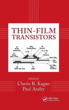
This is a single-source treatment of developments in TFT production from international specialists
Andere Kunden interessierten sich auch für
![Charge Transport Study Of Doped Polymer Thin-film Transistors Charge Transport Study Of Doped Polymer Thin-film Transistors]() Huseynova GunelCharge Transport Study Of Doped Polymer Thin-film Transistors47,99 €
Huseynova GunelCharge Transport Study Of Doped Polymer Thin-film Transistors47,99 €![Semiconducting Metal Oxide Thin-Film Transistors Semiconducting Metal Oxide Thin-Film Transistors]() Semiconducting Metal Oxide Thin-Film Transistors175,99 €
Semiconducting Metal Oxide Thin-Film Transistors175,99 €![FABRICATING SILICON THIN-FILM TRANSISTORS ON PLASTIC AT 300C FABRICATING SILICON THIN-FILM TRANSISTORS ON PLASTIC AT 300C]() Kunigunde CherenackFABRICATING SILICON THIN-FILM TRANSISTORS ON PLASTIC AT 300C52,99 €
Kunigunde CherenackFABRICATING SILICON THIN-FILM TRANSISTORS ON PLASTIC AT 300C52,99 €![Zinc Oxide Thin-Film Transistors Zinc Oxide Thin-Film Transistors]() Divine Khan NgwashiZinc Oxide Thin-Film Transistors39,99 €
Divine Khan NgwashiZinc Oxide Thin-Film Transistors39,99 €![Introduction to Thin Film Transistors Introduction to Thin Film Transistors]() S.D. BrothertonIntroduction to Thin Film Transistors83,99 €
S.D. BrothertonIntroduction to Thin Film Transistors83,99 €![Tunneling Field Effect Transistors Tunneling Field Effect Transistors]() Tunneling Field Effect Transistors150,99 €
Tunneling Field Effect Transistors150,99 €![ZnO Thin-Film Transistors for Cost-Efficient Flexible Electronics ZnO Thin-Film Transistors for Cost-Efficient Flexible Electronics]() Fábio Fedrizzi VidorZnO Thin-Film Transistors for Cost-Efficient Flexible Electronics76,99 €
Fábio Fedrizzi VidorZnO Thin-Film Transistors for Cost-Efficient Flexible Electronics76,99 €-
-
-
This is a single-source treatment of developments in TFT production from international specialists
Produktdetails
- Produktdetails
- Verlag: CRC Press
- Seitenzahl: 544
- Erscheinungstermin: 25. Februar 2003
- Englisch
- Abmessung: 240mm x 161mm x 34mm
- Gewicht: 975g
- ISBN-13: 9780824709594
- ISBN-10: 0824709594
- Artikelnr.: 21820148
- Herstellerkennzeichnung
- Libri GmbH
- Europaallee 1
- 36244 Bad Hersfeld
- gpsr@libri.de
- Verlag: CRC Press
- Seitenzahl: 544
- Erscheinungstermin: 25. Februar 2003
- Englisch
- Abmessung: 240mm x 161mm x 34mm
- Gewicht: 975g
- ISBN-13: 9780824709594
- ISBN-10: 0824709594
- Artikelnr.: 21820148
- Herstellerkennzeichnung
- Libri GmbH
- Europaallee 1
- 36244 Bad Hersfeld
- gpsr@libri.de
Cherie R. Kagan is a Research Staff Member at the IBM T. J. Watson Research Center, Yorktown Heights, New York. The author or coauthor of more than 15 professional publications and holder of four patents with four pending, she is a member of the Materials Research Society, the American Chemical Society, and the American Physical Society. Dr. Kagan received the B.S.E. degree (1991) in materials science and engineering and the B.A. degree (1991) in mathematics from the University of Pennsylvania, Philadelphia, and the Ph.D. degree (1996) in electronic materials from the Massachusetts Institute of Technology, Cambridge. Paul Andry is Research Staff Member at the IBM T. J. Watson Research Center, Yorktown Heights, New York. The author or coauthor of more than 20 professional publications and the holder of two patents with eight pending, he is a member of the Materials Research Society and the Society for Information Display. Dr. Andry received the B.Sc. degree (1986) in physics from the University of Waterloo, Ontario, Canada, the M.Sc. degree (1990) in physics from the Universite de Sherbrooke, Quebec, Canada, and the Ph.D. degree (1997) in materials science from the University of Vermont, Burlington.
Preface, Part I
The Development of and Advances in Amorphous and Polycrystalline Si Materials and Devices, 1. Thin
Film Transistors
A Historical Perspective, 2. Preparation and Properties of Hydrogenated Amorphous Silicon Thin
Film Transistors, 3. Hydrogenated Amorphous Silicon Thin
Film Transistors, 4. Technology of Polysilicon Thin
Film Transistors, 5. Thin
Film Transistors in Active
Matrix Liquid Crystal Displays (AMLCDs), Part II
The Emergence of Alternative Organic Semiconductors and Devices, 6. Organic
Based Thin
Film Transistors, 7. Vacuum
Deposited Organic Thin
Film Field
Effect Transistors Based on Small Molecules, 8. Organic Transistors: Materials, Patterning Techniques and Applications, 9. Polymer Transistor Circuits Fabricated by Solution Processing and Direct Printing, 10. Organic
Inorganic Hybrid Thin
Film Transistors, Index

