Z ZhangFabrication, Properties, and Applications
Van der Waals Heterostructures
Fabrication, Properties, and Applications
Herausgegeben:Zhang, Zheng; Kang, Zhuo; Liao, Qingliang; Zhang, Yue
Z ZhangFabrication, Properties, and Applications
Van der Waals Heterostructures
Fabrication, Properties, and Applications
Herausgegeben:Zhang, Zheng; Kang, Zhuo; Liao, Qingliang; Zhang, Yue
- Gebundenes Buch
- Merkliste
- Auf die Merkliste
- Bewerten Bewerten
- Teilen
- Produkt teilen
- Produkterinnerung
- Produkterinnerung
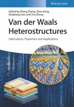
This book systematically introduces the latest developments made in van der Waals heterostructures and devices based on 2D materials in all aspects, from basic synthesis to physical analysis, heterostructures assembling to devices applications.
Andere Kunden interessierten sich auch für
![Graphene for Post-Moore Silicon Optoelectronics Graphene for Post-Moore Silicon Optoelectronics]() Yang XuGraphene for Post-Moore Silicon Optoelectronics90,99 €
Yang XuGraphene for Post-Moore Silicon Optoelectronics90,99 €![Metal Oxide Semiconductors Metal Oxide Semiconductors]() Zhigang ZangMetal Oxide Semiconductors97,99 €
Zhigang ZangMetal Oxide Semiconductors97,99 €![Perovskite Light Emitting Diodes Perovskite Light Emitting Diodes]() Hong MengPerovskite Light Emitting Diodes104,99 €
Hong MengPerovskite Light Emitting Diodes104,99 €![Plasmonic Metal Nanostructures Plasmonic Metal Nanostructures]() Caixia KanPlasmonic Metal Nanostructures119,99 €
Caixia KanPlasmonic Metal Nanostructures119,99 €![Graphene Field-Effect Transistors Graphene Field-Effect Transistors]() Graphene Field-Effect Transistors112,99 €
Graphene Field-Effect Transistors112,99 €![Flexible Electronic Packaging and Encapsulation Technology Flexible Electronic Packaging and Encapsulation Technology]() H MengFlexible Electronic Packaging and Encapsulation Technology105,99 €
H MengFlexible Electronic Packaging and Encapsulation Technology105,99 €![Halide Perovskite Semiconductors Halide Perovskite Semiconductors]() Halide Perovskite Semiconductors119,99 €
Halide Perovskite Semiconductors119,99 €-
-
-
This book systematically introduces the latest developments made in van der Waals heterostructures and devices based on 2D materials in all aspects, from basic synthesis to physical analysis, heterostructures assembling to devices applications.
Produktdetails
- Produktdetails
- Verlag: Wiley-VCH
- Artikelnr. des Verlages: 1134950 000
- 1. Auflage
- Seitenzahl: 336
- Erscheinungstermin: 1. März 2023
- Englisch
- Abmessung: 246mm x 174mm x 20mm
- Gewicht: 782g
- ISBN-13: 9783527349500
- ISBN-10: 3527349502
- Artikelnr.: 63896581
- Herstellerkennzeichnung
- Wiley-VCH GmbH
- Boschstraße 12
- 69469 Weinheim
- wiley-vch@kolibri360.de
Dr. Yue Zhang is the Academician of Chinese Academic Society and a Full Professor of Material Physics at University of Science and Technology Beijing, China. He has authored over 450 scientific publications and is the Chief scientist of National Major Scientific Research Plan and project in China. Dr. Zheng Zhang currently is a full Professor at the School of Materials Science and Engineering and the academy for advanced interdisciplinary science and technology in the University of Science and Technology Beijing. Dr. Zhuo Kang is a full professor at the academy for advanced interdisciplinary science and technology in University of Science and Technology Beijing. Dr. Qingliang Liao is a full professor at the academy for advanced interdisciplinary science and technology in University of Science and Technology Beijing.
1 THE 2D SEMICONDUCTOR LIBRARY
1.1 Introduction
1.2. Emerging 2DLMs for Future Electronics
2 THE 2D SEMICONDUCTOR SYNTHESIS AND PERFORMANCES
2.1 Exfoliation
2.2 Chemical Vapor Deposition
3 THE VDW HETEROSTRUCTURE CONTROLLABLE FABRICATIONS
3.1 Wet Transfer
3.2 Controllable Selective Synthesis
3.3 Dry Transfer
4 THE MIXED-DIMENSIONAL VDW HETEROSTRUCTURES
4.1 Categorization of Mixed-dimensional VdWHs
4.2 Strategies for Constructing Mixed-dimensional VdWHs
4.3 Electronic and Sensing Applications
4.4 Optoelectronic and Photonic Applications
4.5 Energy Applications
4.6 Conclusions
5 THE VDW HETEROSTRUCTURE INTERFACE PHYSICS
5.1 Band Alignment and Charge Transfer in VdWHs
5.2 Magnetic Coupling in VdWHs
5.3 Moiré Pattern
5.4 VdWHs for Protection
5.5 Characterization Techniques for VdWHs
6THE VDW HETEROSTRUCTURE MULTI-FIELD COUPLING EFFECTS
6.1 Introduction
6.2 The Multi-Field Coupling Effect Characterization for 2D Van der Waals Structures
6.3 The Multi-Field Modulation for Electrical Properties of 2D Van der Waals Structures
6.4 The Multi-Field Modulation for Optical Properties of 2D Van der Waals Structures
7 VDW HETEROSTRUCTURE ELECTRONICS
7.1 Van der Waals PN Junctions
7.2 Van der Waals Metal-semiconductor Junctions
7.3 Field-effect Transistor
7.4 Junction Field Effect Transistor
7.5 Tunneling Field-effect Transistor
7.6 Van der Waals Integration
8 VDW HETEROSTRUCTURE OPTOELECTRONICS
8.1 Photodetectors
8.2 Light Emission
8.3 Optical Modulators
9 VDW HETEROSTRUCTURE ELECTROCHEMICAL APPLICATIONS
9.1 Solar Energy
9.2 Van der Waals Heterostructure Application on Hydrogen Energy
9.3 Battery
9.4 Catalyst
9.5 Biotechnology
10 PERSPECTIVE AND OUTLOOK
10.1 Overall Development Status of 2D Materials
10.2 Compatibility between 2D van der Waals device processing and silicon technology
10.3. Promising Roadmap of Van der Waals heterostructure devices [Medium term: 5 years, Long term: 5-10 years]
10.4 Promising Roadmap of Optoelectronic Device
10.5 Conclusion and Prospect

