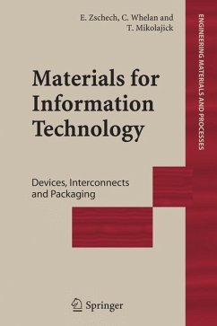
Materials for Information Technology (eBook, PDF)
Devices, Interconnects and Packaging
Redaktion: Zschech, Ehrenfried; Mikolajick, Thomas; Whelan, Caroline
160,95 €
160,95 €
inkl. MwSt.
Sofort per Download lieferbar

80 °P sammeln
160,95 €
Als Download kaufen

160,95 €
inkl. MwSt.
Sofort per Download lieferbar

80 °P sammeln
Jetzt verschenken
Alle Infos zum eBook verschenken
160,95 €
inkl. MwSt.
Sofort per Download lieferbar
Alle Infos zum eBook verschenken

80 °P sammeln
Materials for Information Technology (eBook, PDF)
Devices, Interconnects and Packaging
Redaktion: Zschech, Ehrenfried; Mikolajick, Thomas; Whelan, Caroline
- Format: PDF
- Merkliste
- Auf die Merkliste
- Bewerten Bewerten
- Teilen
- Produkt teilen
- Produkterinnerung
- Produkterinnerung

Bitte loggen Sie sich zunächst in Ihr Kundenkonto ein oder registrieren Sie sich bei
bücher.de, um das eBook-Abo tolino select nutzen zu können.
Hier können Sie sich einloggen
Hier können Sie sich einloggen
Sie sind bereits eingeloggt. Klicken Sie auf 2. tolino select Abo, um fortzufahren.

Bitte loggen Sie sich zunächst in Ihr Kundenkonto ein oder registrieren Sie sich bei bücher.de, um das eBook-Abo tolino select nutzen zu können.
This book provides an up to date survey of the state of the art of research into the materials used in information technology, and will be bought by researchers in universities, institutions as well as research workers in the semiconductor and IT industries.
- Geräte: PC
- ohne Kopierschutz
- eBook Hilfe
- Größe: 13.4MB
Andere Kunden interessierten sich auch für
![Micromachined Thin-Film Sensors for SOI-CMOS Co-Integration (eBook, PDF) Micromachined Thin-Film Sensors for SOI-CMOS Co-Integration (eBook, PDF)]() Jean LaconteMicromachined Thin-Film Sensors for SOI-CMOS Co-Integration (eBook, PDF)112,95 €
Jean LaconteMicromachined Thin-Film Sensors for SOI-CMOS Co-Integration (eBook, PDF)112,95 €![Innovative Superhard Materials and Sustainable Coatings for Advanced Manufacturing (eBook, PDF) Innovative Superhard Materials and Sustainable Coatings for Advanced Manufacturing (eBook, PDF)]() Innovative Superhard Materials and Sustainable Coatings for Advanced Manufacturing (eBook, PDF)160,95 €
Innovative Superhard Materials and Sustainable Coatings for Advanced Manufacturing (eBook, PDF)160,95 €![Materials Chemistry (eBook, PDF) Materials Chemistry (eBook, PDF)]() Bradley D. FahlmanMaterials Chemistry (eBook, PDF)120,95 €
Bradley D. FahlmanMaterials Chemistry (eBook, PDF)120,95 €![Dielectric Polymer Nanocomposites (eBook, PDF) Dielectric Polymer Nanocomposites (eBook, PDF)]() Dielectric Polymer Nanocomposites (eBook, PDF)128,95 €
Dielectric Polymer Nanocomposites (eBook, PDF)128,95 €![Chemical-Mechanical Polishing of Low Dielectric Constant Polymers and Organosilicate Glasses (eBook, PDF) Chemical-Mechanical Polishing of Low Dielectric Constant Polymers and Organosilicate Glasses (eBook, PDF)]() Christopher Lyle BorstChemical-Mechanical Polishing of Low Dielectric Constant Polymers and Organosilicate Glasses (eBook, PDF)112,95 €
Christopher Lyle BorstChemical-Mechanical Polishing of Low Dielectric Constant Polymers and Organosilicate Glasses (eBook, PDF)112,95 €![Modelling of Powder Die Compaction (eBook, PDF) Modelling of Powder Die Compaction (eBook, PDF)]() Modelling of Powder Die Compaction (eBook, PDF)112,95 €
Modelling of Powder Die Compaction (eBook, PDF)112,95 €![Mid-Infrared Coherent Sources and Applications (eBook, PDF) Mid-Infrared Coherent Sources and Applications (eBook, PDF)]() Mid-Infrared Coherent Sources and Applications (eBook, PDF)232,95 €
Mid-Infrared Coherent Sources and Applications (eBook, PDF)232,95 €-
-
-
This book provides an up to date survey of the state of the art of research into the materials used in information technology, and will be bought by researchers in universities, institutions as well as research workers in the semiconductor and IT industries.
Dieser Download kann aus rechtlichen Gründen nur mit Rechnungsadresse in A, B, BG, CY, CZ, D, DK, EW, E, FIN, F, GR, HR, H, IRL, I, LT, L, LR, M, NL, PL, P, R, S, SLO, SK ausgeliefert werden.
Produktdetails
- Produktdetails
- Verlag: Springer London
- Seitenzahl: 508
- Erscheinungstermin: 2. Juli 2006
- Englisch
- ISBN-13: 9781846282355
- Artikelnr.: 37353297
- Verlag: Springer London
- Seitenzahl: 508
- Erscheinungstermin: 2. Juli 2006
- Englisch
- ISBN-13: 9781846282355
- Artikelnr.: 37353297
- Herstellerkennzeichnung Die Herstellerinformationen sind derzeit nicht verfügbar.
Dr Ehrenfried Zschech is manager of the Materials Analysis Department at AMD Saxony LLC & Co. KG in Dresden, Germany. Advanced Microdevices (AMD) is a global manufacturer of microprocessors and other integrated circuit-based products. AMD's manufacturing facility in Dresden is the company's most advanced and the site also hosts the company's European R&D centre. Dr Zschech was the coordinator of the IT topic of EUROMAT 2003 in Lausanne. This book, although not a proceedings, has resulted from his work for the conference. It collects contributions on materials for information technology applications from the author's of conference papers as well as chapters from other authors in order to create a state-of-the art edited volume on the subject from the world's leading experts in academia and industry. Dr Caroline Whelan is a researcher at the Interuniversity MicroElectronics Center (IMEC) Leuven, Belgium, a leading research institution in microelectronics funded by industry, government, ESA and the EU. Dr Thomas Mikolajick is a researcher at Infineon Technologies AG, a German-based IC products manufacturers. Infineon's R&D activities cover innovations in nano technologies, photonics, high frequency circuits, mixed signal circuits, electronic biosensors, systems technology, emerging applications.
Recent Advances in Thin-film Deposition.- Molecular-beam Deposition of High-k Gate Dielectrics for Advanced CMOS.- LEPECVD - A Production Technique for SiGe MOSFETs and MODFETs.- Thin-film Engineering by Atomic-layer Deposition for Ultra-scaled and Novel Devices.- Atomic-layer Deposited Barrier and Seed Layers for Interconnects.- Copper CVD for Conformal Ultrathin-film Deposition.- Pushing PVD to the Limits - Recent Advances.- Surface Engineering Using Self-assembled Monolayers: Model Substrates for Atomic-layer Deposition.- Selective Airgaps: Towards a Scalable Low-k Solution.- Silicides - Recent Advances and Prospects.- TEM Characterization of Strained Silicon.- Material Aspects of Non-Volatile Memories.- An Introduction to Nonvolatile Memory Technology.- Floating-dot Memory Transistors on SOI Substrate.- Ion-beam Synthesis of Nanocrystals for Multidot Memory Structures.- Scaling of Ferroelectric-based Memory Concepts.- Device Concepts with Magnetic Tunnel Junctions.- Phase-change Memories.- Amorphous-to-fcc Transition in GeSbTe Alloys.- Organic Nonvolatile Memories.- Materials for Interconnects.- Interconnect Technology - Today, Recent Advances and a Look into the Future.- Dielectric and Scaling Effects on Electromigration for Cu Interconnects.- Texture and Stress Study of Sub-Micron Copper Interconnect Lines Using X-ray Microdiffraction.- Stress Modeling for Copper Interconnect Structures.- Conductivity Enhancement in Metallization Structures of Regular Grains.- Advanced Barriers for Copper Interconnects.- Synthesis and Characterization of Compounds Obtained by Crosslinking of Polymethylhydrosiloxane by Aromatic Rings.- Revealing the Porous Structure of Low-k Materials Through Solvent Diffusion.- Carbon Nanotube Via Technologies for Future LSIInterconnects.- Nickel Nanowires Obtained by Template Synthesis.- Materials for Assembly/Packaging.- The Importance of Polymers in Wafer-Level Packaging.- Electrically Conductive Adhesives as Solder Alternative: A Feasible Challenge.- The Role of Au/Sn Solder in Packaging.- Packaging Materials: Organic-Inorganic Hybrids for Millimetre-Wave Optoelectronics.- Wafer-Level Three-Dimensional Hyper-Integration Technology Using Dielectric Adhesive Wafer Bonding.- Advanced Materials Characterization.- Challenges to Advanced Materials Characterization for ULSI Applications.- Advanced Material Characterization by TOFSIMS in Microelectronic.- Electronic Properties of the Interface Formed by Pr2O3 Growth on Si(001), Si(111) and SiC(0001) Surfaces.- Materials Characterization by Ellipsometry.- Thermal Desorption Spectrometry as a Method of Analysis for Advanced Interconnect Materials.- Electron Backscatter Diffraction: Application to Cu Interconnects in Top-View and Cross Section.- X-ray Reflectivity Characterisation of Thin-Film and Multilayer Structures.
Recent Advances in Thin-film Deposition.- Molecular-beam Deposition of High-k Gate Dielectrics for Advanced CMOS.- LEPECVD - A Production Technique for SiGe MOSFETs and MODFETs.- Thin-film Engineering by Atomic-layer Deposition for Ultra-scaled and Novel Devices.- Atomic-layer Deposited Barrier and Seed Layers for Interconnects.- Copper CVD for Conformal Ultrathin-film Deposition.- Pushing PVD to the Limits - Recent Advances.- Surface Engineering Using Self-assembled Monolayers: Model Substrates for Atomic-layer Deposition.- Selective Airgaps: Towards a Scalable Low-k Solution.- Silicides - Recent Advances and Prospects.- TEM Characterization of Strained Silicon.- Material Aspects of Non-Volatile Memories.- An Introduction to Nonvolatile Memory Technology.- Floating-dot Memory Transistors on SOI Substrate.- Ion-beam Synthesis of Nanocrystals for Multidot Memory Structures.- Scaling of Ferroelectric-based Memory Concepts.- Device Concepts with Magnetic Tunnel Junctions.- Phase-change Memories.- Amorphous-to-fcc Transition in GeSbTe Alloys.- Organic Nonvolatile Memories.- Materials for Interconnects.- Interconnect Technology - Today, Recent Advances and a Look into the Future.- Dielectric and Scaling Effects on Electromigration for Cu Interconnects.- Texture and Stress Study of Sub-Micron Copper Interconnect Lines Using X-ray Microdiffraction.- Stress Modeling for Copper Interconnect Structures.- Conductivity Enhancement in Metallization Structures of Regular Grains.- Advanced Barriers for Copper Interconnects.- Synthesis and Characterization of Compounds Obtained by Crosslinking of Polymethylhydrosiloxane by Aromatic Rings.- Revealing the Porous Structure of Low-k Materials Through Solvent Diffusion.- Carbon Nanotube Via Technologies for Future LSIInterconnects.- Nickel Nanowires Obtained by Template Synthesis.- Materials for Assembly/Packaging.- The Importance of Polymers in Wafer-Level Packaging.- Electrically Conductive Adhesives as Solder Alternative: A Feasible Challenge.- The Role of Au/Sn Solder in Packaging.- Packaging Materials: Organic-Inorganic Hybrids for Millimetre-Wave Optoelectronics.- Wafer-Level Three-Dimensional Hyper-Integration Technology Using Dielectric Adhesive Wafer Bonding.- Advanced Materials Characterization.- Challenges to Advanced Materials Characterization for ULSI Applications.- Advanced Material Characterization by TOFSIMS in Microelectronic.- Electronic Properties of the Interface Formed by Pr2O3 Growth on Si(001), Si(111) and SiC(0001) Surfaces.- Materials Characterization by Ellipsometry.- Thermal Desorption Spectrometry as a Method of Analysis for Advanced Interconnect Materials.- Electron Backscatter Diffraction: Application to Cu Interconnects in Top-View and Cross Section.- X-ray Reflectivity Characterisation of Thin-Film and Multilayer Structures.
