160,95 €
160,95 €
inkl. MwSt.
Sofort per Download lieferbar
payback
80 °P sammeln
160,95 €
160,95 €
inkl. MwSt.
Sofort per Download lieferbar

Alle Infos zum eBook verschenken
payback
80 °P sammeln
Als Download kaufen
160,95 €
inkl. MwSt.
Sofort per Download lieferbar
payback
80 °P sammeln
Jetzt verschenken
160,95 €
inkl. MwSt.
Sofort per Download lieferbar

Alle Infos zum eBook verschenken
payback
80 °P sammeln
  • Format: PDF

Semiconductor materials have been studied intensively since the birth of silicon technology more than 50 years ago. The ability to physically and chemically t- lor their properties with precision is the key factor responsible for the electronic revolution in our society over the past few decades. Semiconductor material s- tems (like silicon and GaAs-related materials) have now matured and found well established applications in electronics, optoelectronics, and several other ?elds. Other materials such as III-Nitrides were developed later, in response to needs that the above mentioned…mehr

  • Geräte: PC
  • ohne Kopierschutz
  • eBook Hilfe
  • Größe: 10.92MB
Produktbeschreibung
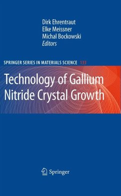
Semiconductor materials have been studied intensively since the birth of silicon technology more than 50 years ago. The ability to physically and chemically t- lor their properties with precision is the key factor responsible for the electronic revolution in our society over the past few decades. Semiconductor material s- tems (like silicon and GaAs-related materials) have now matured and found well established applications in electronics, optoelectronics, and several other ?elds. Other materials such as III-Nitrides were developed later, in response to needs that the above mentioned semiconductors were unable to ful?ll. The properties of I- nitrides (AlN, GaN InN, and related alloy systems) make them an excellent choice for ef?cient light emitters in the visible as well as the UV region, UV detectors, and for a variety of electronic device such as high frequency unipolar power devices. There was a major upsurgein the research of the GaN material system around1970.

Dieser Download kann aus rechtlichen Gründen nur mit Rechnungsadresse in A, B, BG, CY, CZ, D, DK, EW, E, FIN, F, GR, HR, H, IRL, I, LT, L, LR, M, NL, PL, P, R, S, SLO, SK ausgeliefert werden.

Autorenporträt
Dr. Dirk Ehrentraut received a Diploma in Crystallography from the Humboldt University of Berlin, Germany and a Ph.D. in Sciences from the Institute of Applied Optics at the Swiss Federal Institute of Technology in Lausanne (EPFL), Switzerland. He joined the Tohoku University end of 2003 and is currently a visiting professor of the Institute of Multidisciplinary Research of Advanced Materials. His field of competence covers the crystal growth of films and bulk material from the liquid and vapor phase and material aspects of the wide band gap semiconductors of group-III nitrides and ZnO. He has authored 130 publications in books, journals and conferences and holds 6 patents. Dr. Elke Meissner graduated from the University of Erlangen, Germany in the field of applied mineralogy. Later she received a PhD from the University of Bayreuth, Germany. She is a senior scientist in the Department of Crystal Growth at the Fraunhofer Institute of Integrated Systems and Device Technology (IISB) in Erlangen and became head of the working group Defect Engineering in 2007. She has a broad background in process properties correlation for advanced materials in various fields like silicon nitride ceramics and applied & experimental mineralogy. Her recent work is strongly focussed on the structural characterization of crystals and crystal layers of novel semiconductors. Dr. Meissner is inventor or co-inventor of 3 international patents and authored more than 50 papers or contributions to journals and conference. >120 publications in journals and conferences and holds 2 international patents.